1
Feature Story
AI ambition is pushing copper to its breaking point
Nov 28, 2024 · theregister.com
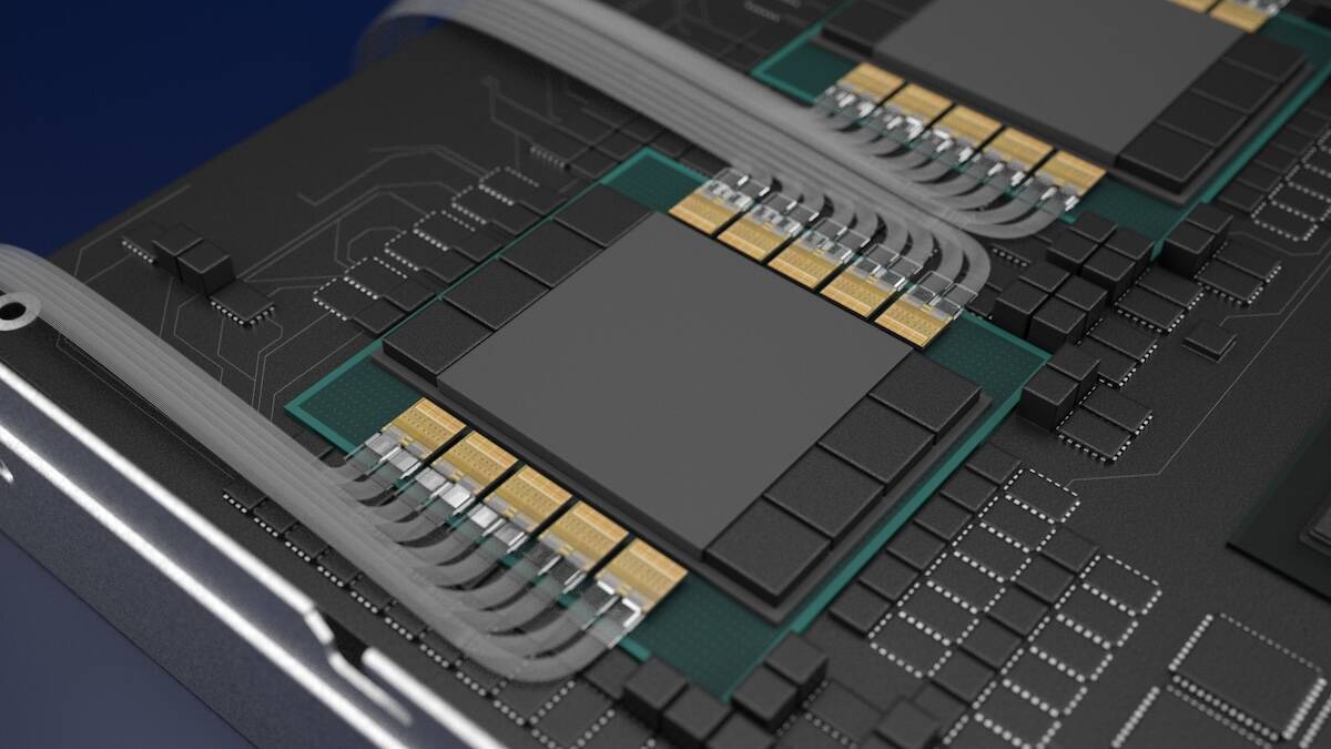
Silicon photonics startup Ayar Labs has been developing an optical interconnect chiplet since 2015, designed to be co-packaged with a CPU or GPU for higher bandwidth over longer distances. This could potentially replace Nvidia's NVLink or AMD's Infinity Fabric to connect multiple chips. The technology could allow a compute and memory domain to stretch across hundreds of GPUs spread among dozens of racks, reducing power and thermal densities per rack. However, challenges remain, including developing a chip that can match existing copper interconnects on power and bandwidth, and developing communication protocols.
Key takeaways
- Datacenters are trending towards denser, more power-hungry systems to support larger AI models, pushing power demands beyond 120 kilowatts in high-density configurations.
- Chip designers like Nvidia use high-speed interconnects to make multiple GPUs behave like a single device, but the faster data is shuffled across a wire, the shorter the distance at which the signal can be maintained.
- Ayar Labs contends that by integrating optics directly into the compute, chipmakers can alleviate bandwidth bottlenecks and lower the rack densities required to support growing model parameter counts.
- Despite the potential of silicon photonics, the technology faces challenges before it can be integrated into production hardware, including developing a chip that can match existing copper interconnects on power and bandwidth, and developing communication protocols.