

1
Feature Story
Take an Early Look at Intel's Glass Packaging Tech for Faster Chips
Sep 18, 2023 · cnet.com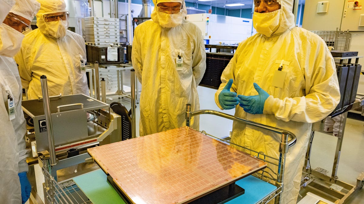
The company uses a variation of lithography machines to etch circuitry onto the glass substrates, creating a complex 3D network for routing data and power signals between a processor and its circuit board. The glass substrate technology is expected to mature later this decade. Intel has also been working on its EMIB (embedded multidie interconnect bridge) technology, which involves tucking tiny silicon bridges under adjoining processor chiplets to serve as a communications link.
Key takeaways
- Intel is developing a glass substrate technology that will improve the performance and power consumption of advanced processors arriving later this decade.
- The glass substrates will allow for physically larger processors made up of several small "chiplets", which will be beneficial for AI and data center work.
- Intel's glass substrate technology involves laying down patterns on the substrates to route data and power signals through a complex 3D network between a processor and its circuit board.
- The technology is being developed at Intel's CH8 facility in Chandler, Arizona, and is expected to replace organic substrates in many situations.